DISCLAIMER
Revision: 0
Date: Aug 23rd, 1997
The digital effects page
 Delay, echo, reverb
- The block diagram is easy, a bit more complicated than the analog one, due
to more timings to deal with. We'll have, as expected, an antialias filter
at the input, an A/D converter, a memory block which will implement the
delay itself, and an interpolation filter at the output, to reconstruct the
analog signal, and to limit the high frequency response in the case of the
echo effect.

I basically know two kinds of systems, the choice
between one them depends on the A/D D/A method to use. Should we choose
the CVSD (Continuously Variable Slope Delta Modulation) method, we'll get a
serial data stream in which each data bit represents the interpolation
slope to the last signal value; so the memory will have to be organized as
a big shift register, with a serial input and a serial output. The delay
time depends on the sampling frequency and the memory block lenght, in
bits. As we already know, a CVSD based A/D converter can't operate at
Nyquist rate, so the lowest operating frequency will depend on the lowest
signal to noise ratio we can tolerate, and the highest working frequency
will depend on the quality and technology of the different components
(memory access time, comparator speed, etc.). The delay so obtained is the
shift register lenght multiplied by the clock period.
The other system uses a standard parallel converter, so the converted data
represents the signal value at that time, in the discrete scale
corresponding to the converter´s word lenght. This can be of any technology
(flash, SAR, sigma-delta), as long as the output data corresponds to the
given description.
The read data is transferred to the memory in parallel
(the memory is constructed as a circular buffer), and then, data at another
location is read and sent to the output. The delay time is the difference
between both memory locations, so, if I write at location 2000 and read
from location 1000, I'm reading a data that was written 1000 clock periods
ago. Same situation arises when writing at location 500 and reading from
location 2500 on a 3000 words buffer. So, the delay time is calculated as
the difference between the reading and writing locations multiplied by the clock
period.
The used clock, in both systems, will have to be a multi-phase clock,
in order to select the start of conversion , data read, data write, pointer
actualization, etc.
The reverberation effect this system produces has no realism, sounding
sometimes "steel-like"; so I recommend the plate
system.
 Flanger, Chorus
- Once the delay system is built (as explained on last
paragraph), delay time can be modulated to achieve flanger or chorus
effects, replacing the clock oscillator with a VCO, modulated by an LFO
(Low Frequency Oscillator), preferably of a triangular waveshape for the
flanger and a sinewave for the chorus, although the triangular gives
also a good chorus effect with a good signal to noise ratio.

 Pitch shift
- It is actually feasible to build one of this gremlins with a chorus, by changing the LFO waveshape to a linear sawtooth.
Although the obtained effect is not quite pleasing. A two chorus
(counter-phase) implementation is theoretically possible, although I
haven't tried it myself, and I don't believe that these techniques would
be appropiate for this job.
 Additional explanations
 Delta Modulation and CVSD
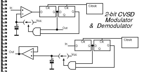
- A/D conversion by means of delta modulation means to aproximate the analog
signal with a slope, generated (for example) by charging a capacitor. If
the slope excedes the signal value at the time signalled by the clock, then
the slope sign is inverted. The value obtained is the comparator output,
which is the sign of the slope. Essentially, this system codes the analog
signal mean (during the sampling interval) into the comparator output pulse
width; so the D/A conversion is easily done with an RC integrator fed by
the last data (generally, a circuit which is similar to the A/D is used).
This has its own problems, as we can see, we have to work at a frequency
much higher than the signal's, so the slope can follow it. If the signal
rises faster than the slope, it can not follow it. Furthermore, in the
absence of input signal, the slope alternates signs.

To avoid these problems, memory and CVSD are introduced. The slope is
continually modified, based on the last 2/3/4 values, so if the signal
rises too fast, the slope is increased; if it doesn't change very much,
the slope is decreased. The CVSD demodulation requires reproduction of the
A/D circuitry at the output, integrating the resulting slope.

There exist some commercial ICs that implement this conversion technique,
although I couldn't get hold of any of them to experiment with.
Nevertheless, I have built and tested a discrete version, with pleasing
results.
 Memory as a shift register
- Using memories with data-in and data-out pins, a long shift register can
be built.
These pins are cascaded, output to input, leaving the first memory's
data-in as the input and the last one data-out as the output. A counter
will generate addresses at each clock pulse, driven by a multi-phase
clock, which will also generate the read and write pulses, and the RAS and
CAS pulses in case of dynamic memories being used. So, on each clock
pulse, a data bit is written to a memory location, and C counts later (C
is the number of counts the counter performs before repeating its cycle),
it is output on the data-out pin, to be written to the following memory.
This way, the data seems to advance one memory location each clock pulse, passing through the
chips, until it is output at the last one, N clock periods later, where N
is the total memory lenght.

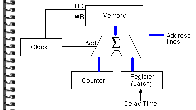
 Circular buffer
- This is easily accomplished with a counter generating memory address
lines. Nevertheless, the buffer lenght must be a power of two (2 to the
number of address lines). The address so pointed will be, for example, the
write address; which will be incremented any time the counter advances.
The difference between the read and write addresses is often stored in a
register, which will in time be added to the counter to obtain the new
address, in this case, the read address.

This page hosted by  Get your own Free Home Page
 Delay, echo, reverb
 Flanger, Chorus
 Additional explanations


