DISCLAIMER
Revision: 0
Date: Aug 23rd, 1997
The analog effects page
 Delay, echo, reverb
- A delay can be easily built by using an analog BBD
delay line; reverberation generated in this way is very poor, as it has no
realism. For a good reverb sound, I recommend the plates'
system.
I'm not going to discuss Nyquist's sampling theorem, let it
suffice that we must sample at a frequency higher than the highest
component of our signal source.
In the guitar case, we can lower the
bandwith down to 5 or 6 KHz, so a 10/12 KHz signal will be our clock´s
minimum rate, providing a maximum delay of around 25 ms. on a TDA1022 (too
short) and around 250 ms. on a MN3005. As an echo, these delay is pretty
short, but it lets us produce some delay effects at least. The best delay
is achieved by using an endless tape system.
The block diagram is easy, signal goes first to an antialias filter, which limits its
bandwidth to half the clock's frequency; then goes into the delay line. The
output is further filtered to eliminate the clock residuals and is then fed
back to the input to achieve the repetition effect, and is added with the
original signal at the output before leaving.
To enhance the otherwise poor BBD´s signal to noise
ratio, sometimes a compandor is inserted
in the path, in order for the delay line to work with stronger signals.
The delay time is adjusted varying the clock's frequency.

 Flanger
- Flanger's construction is identical to delay, except
that to achieve the variable delay, the clock oscillator is replaced with a
VCO, which is modulated by an LFO (Low Frequency Oscillator); whose signal
should be preferably triangular.
It is because of the problems inherent to BBD lines, that
the flanging effect so obtained is pretty weak, being digital or DSP
implementations a bit better. The BBD used should have few
stages in order to achieve shorter delays, and a maximum of 10 ms. The
TDA1022 chip is not often the best choice, but it works. I've seen some
circuits using the MN3007 chip, but I couldn't get any information on that
chip.

 Chorus
- The chorus schematic is identical to the flanger's,
except that feedback is removed, and the LFO gives better results if its
waveshape is a sine.
Even with the BBD inherent
problems, the chorus effect so obtained is pretty good, although of an
inferior quality than a digital or DSP implementation.
The TDA1022 chip is a very nice BBD to build a chorus, as
long as the 25 ms. delay time is not exceeded. The MN3005 chip gives a
longer delay, sometimes too long, but it has the advantage of letting one
work with a higher bandwidth for the same delay time.
 Pitch shift
- It is actually feasible to build one of this gremlins with a chorus, by changing the LFO waveshape to a linear sawtooth.
Although the obtained effect is not quite pleasing. A two chorus
(counter-phase) implementation is theoretically possible, although I
haven't tried it myself, and I don't believe that analog techniques would
be appropiate for this job.
 Reverberation
- An excelent reverberation chamber can be achieved with a couple of
different lenght (and k) plates, connected to a pair of transducers. The
input transducer is fed with a power amplifier's output (0.5W will
suffice), and so it transfers the excitation to the plates. On the other end,
the signal is picked up with the remaining transducer and fed to a
diferential amplifier, to avoid buzz. Bass frequencies should be somehow
attenuated before going to the exciter amplifier, and the diferential pick
up should be conveniently equalized. This is because the transducers are
coils, which are inductors. We are exciting an inductor with a voltage
source, so the current flowing through it will induce a magnetic flux that
will in turn move a magnetic piece connected to the plate. This flux will
be directly proportional to the current, and the current will be inversely
proportional to the frequency, so, in order to compensate for this, the
excitation amplifier should have a transfer function which is directly
proportional to the frequency (at least inside the needed audio range). On
the output, the reverse situation occurs, as now the magnetic piece moves
inside a magnetic field, and induces a voltage which is proportional to
the flux variation derivative, which implies a direct dependence of
frequency, as d(sin(wt))/dt = w cos(wt). Because of constructive reasons,
this behaviour is somehow attenuated, so a straight 1/f transfer is
not needed. Experimentation with that particular chamber should be the
best choice.
 Echo
Echo
- The best echo is buillt with a 3 head tape recorder and an endless
tape: one head erases, another one records, and the third one plays. The
echo's delay time is determined by the time it takes for the tape to go
from the recording head to the playback head (which can be the whole tape
lenght if the playback head is located before the recording head). The delay time
is set by altering the tape travelling speed.
 Compression, expansion , compression-expansion, compressor/limiters, downward expanders and noise-gates.
- There are some embedded chips that implement the compression/expansion
function, as the NE570/1/2 series, however, they are not well suited for
compressor/limiters and downward expanders or noise gates.
To build one of these effect boxes, an analog circuit performing the log
function is needed, in order to get the dB value of the input signal. This
is quite difficult, as these kind of circuits work using the
diode/transistor exponential transfer characteristic, which is in itself
temperature dependent.
The gain reduction stage implies the need for a voltage controlled
attenuator or a VCA. A FET as a controlled resistor can be
used, but an OTA (Operational Transconductance Amplifier) based VCA is
often a better choice.
There are some ICs as Analog Devices' SSM2120, which perform all the
necessary functions in a single chip. Discrete implementation is possible,
but it gets complicated, I still haven't got the time to test mi discrete
development on this field.
A very simple solution, if extreme precision is not required, could be to
connect a FET as a variable resistor on an operational
amplifier's feedback loop, and control it with the integrated peaks of the
output signal. So, the
FET will reduce the amp's gain when the signal increases, and increase the
gain when the signal reduces.
 Phaser or phase shifter
- The phaser is built with a group of cascaded phase shifting
stages, 4 or 6 are enough. The phase shift variation is achieved replacing the R
resistor with a FET, which is itself controlled by an LFO (Low Frequency
Oscillator). This FET, connected as a variable resistor,
needs a low level signal to avoid generating excessive distortion, so this
circuit tends to distort with strong signals. The LFO is often a sawtooth,
to compensate for the FET's variation law; ending up as an acceptable
approximation.
 Additional explanations
 BBD delay line
- A BBD delay line is a chain of capacitors interchanging charges at a
pace set by a clock signal. BBD means Bucket Brigade Delay, and it is an
analogy between the charge interchange and a lot of buckets interchanging
water, where the water represents the electric charges. A bucket in the
last stage is filled up with water, and the bucket in the first stage is
filled with the input signal level. At clock time, all the buckets´contents
are dropped into its partner, from output to input. Let's suppose we have two
buckets: bucket #1 is filled with the signal source, and bucket #2 is
filled up. When bucket #2's contents are dropped into bucket #1, it fills
up, so bucket #2 now has bucket #1's level, as bucket #2 gave bucket #1 the
difference to fill it up. By extending the number of buckets, we understand
how this delay works.
The delay so obtained, depends on the number of stages (capacitors), and
the clock's frecuency: Td = #stages / Fclock. There are commercial chips
like the TDA1022 with 512 stages, the MN3005, and some more I could never
get hold of...
Essentially, the clock needed is often a two phase one, so the obtained
delay is Td = #stages / (2 * Fclock).
Commonly, they can't work with an Fclock higher than 1MHz, and before this
limit they start to distort the signal, due to the time employed by the
capacitors in the charge transfer process.
Its dynamic range is pretty reduced, as the output noise is quite high and
the maximum input signal is often restricted to Vcc/3. A TDA1022 chip gives
a minimum delay of approx. 500 usec., but signal amplitud is quite low, and
distorsion is quite high.
 Logarithmic amplifier
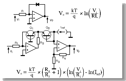
- A diode in an operational amplifier's feedback loop solves this
problem: the diode's characteristic equation is Id = Is * e ^ (Vd *
q/kT),
and so the circuit outputs Vo = Vd = kT/q * ln( Vi / (R * Is)), as Id =
Vi/R.
The problem we have here is that not only this circuit is highly
temperature dependent, but the term R * Is makes the result practically
unusable, introducing a strong dependence to constructive parameters and
also temperature...
We therefore introduce another solution, a matched transistor pair,
connected by its emitters; so, knowing that Ic = Is e ^ (Vbe * q/kT), then
results Vo = kT/q * (R4/R3 + 1) * ( ln(Vi / R1) - ln(Iref)). This way,
setting for (R4/R3 +1) to have a 1/T slope (by inserting a thermistor), we
can compensate the thermal drift the kT/q term introduces.
Glossary: k is Boltzmann's constant; q is the electron's
charge; T is the absolute temperature; Is is the inverse
saturation current.

 FET as a variable resistor
- With small drain-source signal values (less than 300 mV), the circuit
in the figure presents a drain-source resistance inversely proportional to
the control voltage's square root. The feedback network is introduced to
eliminate second harmonic distorsion, introducing third harmonic
distorsion, but in a lesser grade; becoming aceptable on the indicated
signal levels. The only condition is that R be much bigger than the maximum
rds, and also C's capacitive reactance be much smaller than
R, at working
frecuency. The name 'ron' is given to the resistance rds measured at zero
control voltage. Vp is the FET's cut-off voltage, and as
ron, is a constructive parameter.

This page hosted by  Get your own Free Home Page
 Delay, echo, reverb
 Flanger
 Chorus
 Pitch shift
 Reverberation
 Echo
Echo Compression, expansion , compression-expansion, compressor/limiters, downward expanders and noise-gates.
 Additional explanations
